
Discovered Materials Offers $1 Million to Solve AI Chip Manufacturing Challenges
Backed by Y Combinator, the startup aims to bypass physical limits in semiconductor development by offering cash prizes for scientific challenges stalling AI scalability.
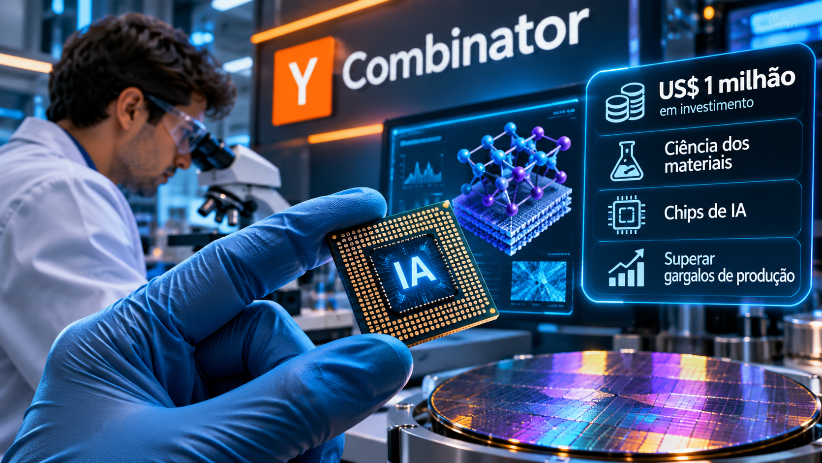
Startup linked to Y Combinator bets $1 million on materials research to overcome technological limitations in semiconductor production used in artificial intelligence.
The Story in 1 Minute
- A startup Discovered Materials, integrante do programa Y Combinator, anunciou um aporte de US$ 1 milhão dividido em cinco desafios científicos.
- A Discovered Materials, startup incubada pela Y Combinator (YC), formalizou uma iniciativa estratégica para acelerar o desenvolvimento de semicondutores através da ciência dos materiais.
- A empresa anunciou a alocação de US$ 1 milhão para financiar soluções de cinco problemas teóricos ainda não resolvidos no setor.
Discovered Materials, a startup incubated by Y Combinator (YC), has formalized a strategic initiative to accelerate semiconductor development through materials science. The company announced the allocation of $1 million to fund solutions for five yet-unsolved theoretical problems in the sector. Each validated solution will be awarded a $200,000 prize. The initiative is a rare example of direct private capital allocation for basic research in a sector where the hardware development cycle is historically slow, expensive, and financed mostly by giants like NVIDIA, Intel, and TSMC.
This move reflects a critical inflection point in the race for artificial intelligence leadership: the physical limits of hardware. As the computational demands of large language models (LLMs) grow exponentially, current silicon-based architecture faces challenges in thermal dissipation, energy efficiency, and processing speed. Discovered Materials' bet suggests that the next phase of performance gains will not come solely from software or logic circuit design, but from molecular innovations in conductive and insulating materials used in chip foundries.
Context and Economic Scenario
The semiconductor sector operates under a capital-intensive logic, with the CAPEX (capital expenditures) of new chip factories, known as fabs, easily reaching tens of billions of dollars. Materials science is often the hidden bottleneck in this ecosystem; the discovery of a new compound enabling more efficient chips can alter the marginal production cost curve of global data center infrastructure. Currently, reliance on traditional discovery methods based on trial and error in physical laboratories limits the speed of innovation.
Discovered Materials' approach uses artificial intelligence to simulate and predict the behavior of new materials, drastically reducing the time between theoretical hypothesis and experimental validation. This method, often referred to as AI for Science, is attracting increasing volumes of venture capital. By decentralizing part of this research, the company aims to avoid the risk of intellectual property concentration and leverage the collective intelligence of the global scientific community to resolve specific impasses the chip industry faces during the transition to process nodes below 2 nanometers.
The current macroeconomic scenario, marked by high interest rates in developed economies and the urgent need to boost productivity via AI, places pressure on technology companies to deliver tangible results in reducing energy consumption. Using AI to discover new materials is not just a quest for computational performance; it is an energy efficiency strategy. More efficient chips mean data centers with lower operating costs and a smaller carbon footprint, crucial factors for the long-term financial viability of AI infrastructure.
How This Affects Your Wallet and Investors
For technology sector investors, the initiative signals a paradigm shift in the expected ROI (return on investment) from semiconductor companies. Traditionally, manufacturers' market value is tied to their scale and market leadership capacity. Projects like Discovered Materials indicate that companies capable of integrating AI into the R&D (research and development) cycle can secure lasting competitive advantages, drastically reducing the time-to-market innovation cycle.
For citizens and the real economy, although the impact may seem distant, resolving these material bottlenecks will eventually enable the viability of more accessible, cheaper, and powerful AI technologies integrated into everyday devices. The fiscal stability of leading technology nations ultimately depends on maintaining this competitive advantage in advanced manufacturing. Any advance in materials science that reduces dependence on scarce inputs or inefficient energy processes strengthens the resilience of the global technology supply chain.
Developments and Next Steps
The success of this initiative depends on the scientific community's ability to deliver solutions that are technically viable for industrial scale. The $1 million figure, while relevant for an early-stage startup, is symbolic compared to the multibillion-dollar R&D budgets of industry leaders. Real impact will be measured by the technical feasibility of the proposed innovations and the speed with which larger players incorporate them.
Investors and analysts should monitor not only the outcome of these five challenges, but also whether the "innovation prize" model will be adopted by other companies in the YC ecosystem and beyond. Open collaboration to solve fundamental scientific problems could become a new efficiency metric for deep tech startups, serving as an indicator of agility in solving complex problems that stall entire sectors of the global economy.
What this means for you
This method, often referred to as AI for Science, is attracting increasing volumes of venture capital.
This contextual analysis is strictly educational and informational regarding macroeconomic trends. It does not constitute investment advice.
This story was originally investigated and reported in Brazil. Numerical figures and data remain preserved in their official units.